Engineering Semiconductor Nanostructures Using Plasmas
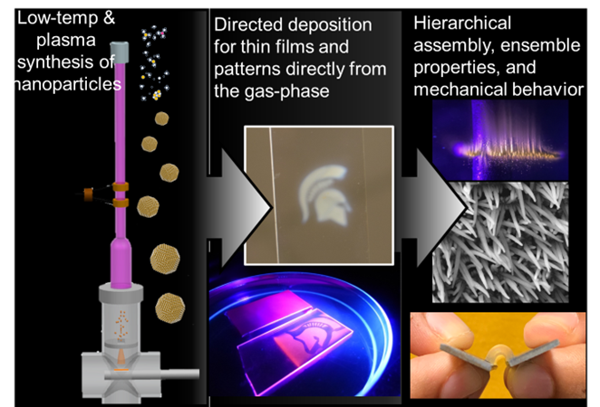
This project involves hands-on synthesis and characterization of semiconductor nanostructures using nonthermal plasma reactors. Semiconductor nanostructures, such as silicon nanocrystals, few-layer-graphene quantum dots, and Group III-V semiconductor nanoparticles, can exhibit new and exciting physical and optoelectronic properties. Plasma reactors are versatile tools for making thin films of semiconductor nanostructures with controllable characteristics. During the 10 week program, the student, together with a graduate student mentor, will conduct synthesis experiments using the reactor, as well as using in-situ diagnostics to understand plasma properties. The student will then characterize the synthesized nanostructures using measurement techniques such as photoluminescence spectroscopy (PL), Raman spectroscopy, x-ray diffraction (XRD), transmission and scanning electron microscopy (TEM/SEM), and Fourier-transform infrared spectroscopy (FTIR). The student will be responsible for analyzing the results, presenting them during the weekly group meetings, and presenting a poster on their work at the Mid-Michigan Symposium for Undergraduate Research Experiences (Mid-SURE).
Scientific goals:
- Unravel process-nanostructure-property relationships for plasma-produced semiconductor nanostructures
- Use in-situ diagnostics on the plasma together with nanostructure characterization to build up a physical understanding of how to control nanostructure properties.
Student learning goals:
- Learn plasma physics/processing principles for flow-through, nonthermal plasma reactors
- Understand the significance of in-situ diagnostics on the reactor
- Tie together the processing parameters (via diagnostics) and the resulting nanostructure properties for functional use in applications