
Sustainable Energy Systems

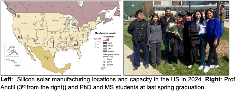
Environmental impact of semiconductor manufacturing for solar applications
- Identify material availability from primary and recycled sources for solar manufacturing.
- Our ultimate goal is to understand the environmental impact of solar semiconductor manufacturing in the US and the impact of primary and recycled semiconductor production. Learn more
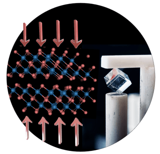
Plasmas and Nanomaterials

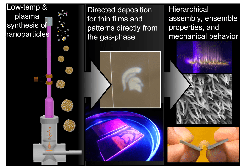
Engineering Semiconductor Nanostructures Using Plasmas
- Unravel process-nanostructure-property relationships for plasma-produced semiconductor nanostructures
- Use in-situ diagnostics on the plasma together with nanostructure characterization to build up a physical understanding of how to control nanostructure properties. Learn more
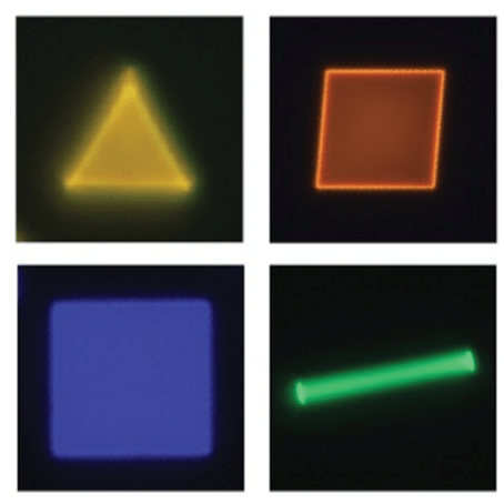
NanoPhotonics and Energy Materials

Synthesis and X-Ray Characterization of Hybrid Semiconductor Materials
- Develop methods to synthesize new hybrid semiconductor materials
- Use X-ray diffraction characterization to analyze materials to verify their identity and structural properties
- Our goal is to synthesize new hybrid semiconductor materials with novel properties and analyze their structural and optical characteristics to find a correlation between crystal structure and optoelectronic properties, as well as determine their potential in optoelectronic devices. Learn more
AI QUANTUM Lab

Designing Semiconductors with Supercomputers and cutting-edge quantum computational techniques
- Understanding Material Properties Using Quantum Computational Techniques: Predict and analyze the physical and chemical properties of diamond and diamond-doped materials using density functional theory (DFT). This can lead to the design of materials with tailored characteristics, such as enhanced hardness or improved electrical conductivity.
- Atomic-Level Mechanisms of Diamond Growth: Investigate the atomic-level processes involved in the growth of diamonds. Simulating how atoms interact and arrange themselves during diamond formation will provide insights that could optimize and control the growth process, which is crucial for various industrial applications.
- Advancing Semiconductor Material Discovery: Utilize and further develop a novel high-throughput computational method to discover and optimize semiconductor materials for applications in artificial photosynthesis and solar energy conversion. This work aims to accelerate breakthroughs in sustainable energy technologies. Learn more
Diamond and Quantum Materials

Characterizing electrical transport in doped diamond for quantum applications
- Analyzing doped diamond for its electrical properties including the conductivity and carrier mobility
- Our ultimate goal is to fabricate p-i-n diode structures using optimized growth recipes for tuning the charge state of defect qubits in diamond. Learn more
Boron-Doped Diamond Solutions (Fraunhofer CMW)

Creating robust electrochemical sensors for biological and environmental monitoring
- Packaging of diamond sensors
- Robust surface activation for long-term measurements
- Characterization of sensor response with coatings and surface modifications. Learn more
Novel Quantum Materials
Crystal Growth of Low Dimensional Quantum Materials with Charge Density Waves
- Investigate the factors that stabilize superconductivity and charge density waves (CDWs) in low-dimensional materials.
- Define the relationships between crystal structures, chemical bonding interactions, CDWs, and superconductivity, aiming to uncover how these elements collectively influence the material’s electronic properties. Learn more
Advanced Materials for Thermal Energy Conversion

Engineering thermal transport in semiconductors for thermoelectric applications
- Combining these thermal conductivity with speed of sound measurements allows us to interpret trends in thermal conductivity as a function of composition, crystal structure, and temperature.
- Our ultimate goal is to understand how the crystal structure (atomic arrangement) in semiconductors controls their ability to conduct heat, especially at high temperatures. Learn more
Analysis of Defect Dynamics in Semiconductor Devices

Characterization and Analysis of Defect Dynamics in Semiconductor Devices
Modern RF power amplifier modules employ compound semiconductors for their superior performance. However, the main disadvantage of compound semiconductor-based power amplifier transistors, specifically gallium nitride (GaN) high electron mobility transistors (HEMTs), is semiconductor defects which degrade electrical performance and can result in transistor reliability issues. This project will involve characterization and analysis of defects, also called traps, in GaN HEMTs.
Synthesis of Emerging Semiconductors via “Sulfurization”

Synthesis of emerging metal-chalcogenide semiconductors
This project is focused on the synthesis of a new class of semiconductors, the chalcogenide perovskites. Chalcogenide perovskites are an interesting group of materials that are highly stable and made from earth-abundant and non-toxic elements. The development of chalcogenide perovskites could lead to cheap, safe, and sustainable semiconductor devices like solar cells or LEDs. But so far, most researchers have focused only on a single chalcogenide perovskite, BaZrS3. This project will focus on creating new sulfide perovskites, first by synthesizing the analogous oxide perovskites and then by converting the oxides into sulfides through “sulfurization.”
Early Engagement in Semiconductor Materials and Technologies

Research Experience for Undergraduates (REU) at MSU
